
Berkeley Lab researchers have found a 3D analogue of the cutting-edge 2D material graphene. It could revolutionize the high tech industry, bringing things like much faster, far more compact hard drives, and paving way for new electronic technologies.
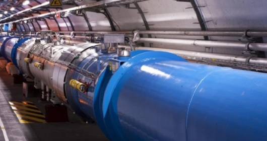
Researchers at the US Department of Energy’s Lawrence Berkeley National Laboratory have announced the discovery of a compound that can exist as a form of quantum matter known as the three-dimensional topological Dirac semi-metal (3DTDS).
The research team supported by the DOE Office of Science and the National Science Foundation of China used sodium bismuthate to produce this novel state, the very existence of which had been proposed by theorists fairly recently. The discovery comes less than a decade after graphene, the thinnest and the strongest known stable material with amazing conductivity of electricity and heat was isolated by UK-based, Russian-born scientists, Andre Geim and Konstantin Novoselov.
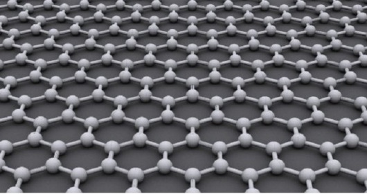
Although dubbed a “wonder material,” graphene has not yet seen an applicable use on an industrial scale. The reason for that lies in its ground-breaking properties and structure, being a two-dimensional, one-atom thick layer of graphite.
“Ever since graphene was isolated in 2004, researchers around the world have looked for ways to take full advantage of its many desirable properties. But the very thing that makes graphene special – the fact that it consists of a single layer of atoms – sometimes makes it difficult to work with, and a challenge to manufacture,” explains Yulin Chen, a physicist with Berkeley Lab’s Advanced Light Source (ALS).

Image from sciencemag.org
However, the potential of the new material has fascinated scientists and governments alike, with thousands of research papers on graphene written since 2005 and numerous research groups created in the UK, the US, Europe, Japan, China, Russia. The EU promised to support the research of graphene with 1 billion euro ($1.3bn) if it can yield practical results in the fields of electronics, energy, health and construction.
While some developed a way to produce semi-transparent, ultra-thin and ultra-light graphene tape, others, including the Berkeley Lab group, focused on looking for means of enclosing graphene’s properties into a three-dimensional material.
Chen, who initiated the discovery, now states that “a 3DTDS is a natural three-dimensional counterpart to graphene with similar or even better electron mobility and velocity.”
The material’s properties feature magnetoresistance “orders of magnitude higher than the materials now used in hard drives” – a potential breakthrough for computer technologies. It also “opens the door to more efficient optical sensors,” Chen adds.
Unfortunately, sodium bismuthate, whose electronic structure was tested at the lab’s ASL facility, is too unstable to be used in devices without proper packaging. But having proved that a 3D structure can actually have comparable or even better features of graphene, the scientists are now extremely keen to explore and develop sturdier 3DTDS materials.
If developed, they will provide “a significant improvement in efficiency in many applications,” while being “easier to fabricate,” Chen stresses, hinting that future electronic technologies are close to reality.
[sc:ad-text]
Source: www.rt.com
[sc:end t=”Hi-tech Gamechanger: Newly-discovered ‘3D graphene’ May Lead to Electronics Revolution”]


Comments are closed.